I:=I*5+2; before I:=J; in the following sequence:
	I := J;
	I := I * 5 + 2;
Clearly we need some way to control which statement executes first and which executes second.
J into I takes a certain amount
of time. Likewise, multiplying I by five and then adding two
and storing the result back into I takes time. As you might
expect, the second Pascal statement above takes quite a bit longer to execute
than the first. For those interested in writing fast software, a natural
question to ask is, "How does the processor execute statements, and
how do we measure how long they take to execute?" CPUs are a good example of a complex synchronous logic system (see the
previous chapter). The system clock gates many of the logic gates that make
up the CPU allowing them to operate in a synchronized fashion.
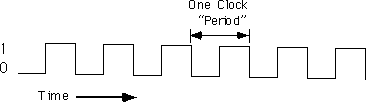
The frequency with which the system clock alternates between zero and one
is the system clock frequency. The time it takes for the system clock
to switch from zero to one and back to zero is the clock period. One
full period is also called a clock cycle. On most modern systems,
the system clock switches between zero and one at rates exceeding several
million times per second. The clock frequency is simply the number of clock
cycles which occur each second. A typical 80486 chip runs at speeds of 66million
cycles per second. "Hertz" (Hz) is the technical term meaning
one cycle per second. Therefore, the aforementioned 80486 chip runs at 66
million hertz, or 66 megahertz (MHz). Typical frequencies for 80x86 parts
range from 5 MHz up to 200 MHz and beyond. Note that one clock period (the
amount of time for one complete clock cycle) is the reciprocal of the clock
frequency. For example, a 1 MHz clock would have a clock period of one microsecond
(1/1,000,000th of a second). Likewise, a 10 MHz clock would have
a clock period of 100 nanoseconds (100 billionths of a second). A CPU running
at 50 MHz would have a clock period of 20 nanoseconds. Note that we usually
express clock periods in millionths or billionths of a second.
To ensure synchronization, most CPUs start an operation on either the falling
edge (when the clock goes from one to zero) or the rising edge
(when the clock goes from zero to one). The system clock spends most of
its time at either zero or one and very little time switching between the
two. Therefore clock edge is the perfect synchronization point.
Since all CPU operations are synchronized around the clock, the CPU cannot
perform tasks any faster than the clock. However, just because a CPU is
running at some clock frequency doesn't mean that it is executing that many
operations each second. Many operations take multiple clock cycles to complete
so the CPU often performs operations at a significantly lower rate.
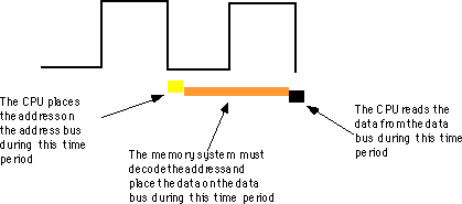
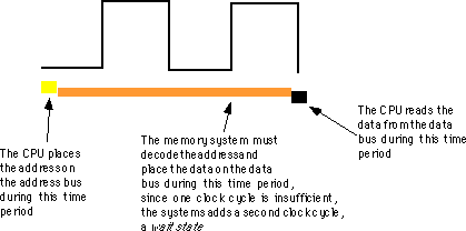
Writing data to memory is similar to:
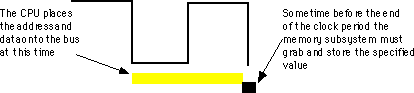
Note that the CPU doesn't wait for memory. The access time is specified
by the clock frequency. If the memory subsystem doesn't work fast enough,
the CPU will read garbage data on a memory read operation and will not properly
store the data on a memory write operation. This will surely cause the system
to fail.
Memory devices have various ratings, but the two major ones are capacity
and speed (access time). Typical dynamic RAM (random access memory) devices
have capacities of four (or more) megabytes and speeds of 50-100 ns. You
can buy bigger or faster devices, but they are much more expensive. A typical
33 MHz 80486 system uses 70 ns memory devices.
Wait just a second here! At 33 MHz the clock period is roughly 33 ns. How
can a system designer get away with using 70 ns memory? The answer is wait
states.
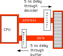
In this diagram, the system loses 10ns to buffering and decoding. So
if the CPU needs the data back in 20 ns, the memory must respond in less
than 10 ns.
You can actually buy 10ns memory. However, it is very expensive, bulky,
consumes a lot of power, and generates a lot of heat. These are bad attributes.
Supercomputers use this type of memory. However, supercomputers also cost
millions of dollars, take up entire rooms, require special cooling, and
have giant power supplies. Not the kind of stuff you want sitting on your
desk.
If cost-effective memory won't work with a fast processor, how do companies
manage to sell fast PCs? One part of the answer is the wait state. For example,
if you have a 20 MHz processor with a memory cycle time of 50 ns and you
lose 10 ns to buffering and decoding, you'll need 40 ns memory. What if
you can only afford 80 ns memory in a 20 MHz system? Adding a wait state
to extend the memory cycle to 100 ns (two clock cycles) will solve this
problem. Subtracting 10ns for the decoding and buffering leaves 90 ns. Therefore,
80 ns memory will respond well before the CPU requires the data.
Almost every general purpose CPU in existence provides a signal on the control
bus to allow the insertion of wait states. Generally, the decoding circuitry
asserts this line to delay one additional clock period, if necessary. This
gives the memory sufficient access time, and the system works properly
Sometimes a single wait state is not sufficient. Consider the 80486 running
at 50 MHz. The normal memory cycle time is less than 20 ns. Therefore, less
than 10 ns are available after subtracting decoding and buffering time.
If you are using 60 ns memory in the system, adding a single wait state
will not do the trick. Each wait state gives you 20 ns, so with a single
wait state you would need 30 ns memory. To work with 60 ns memory you would
need to add three wait states (zero wait states = 10 ns, one wait
state = 30 ns, two wait states = 50 ns, and three wait states = 70 ns).
Needless to say, from the system performance point of view, wait states
are not a good thing. While the CPU is waiting for data from memory
it cannot operate on that data. Adding a single wait state to a memory cycle
on an 80486 CPU doubles the amount of time required to access the
data. This, in turn, halves the speed of the memory access. Running
with a wait state on every memory access is almost like cutting the processor
clock frequency in half. You're going to get a lot less work done in the
same amount of time.
You've probably seen the ads. "80386DX, 33 MHz, 8 megabytes 0 wait
state RAM... only $1,000!" If you look closely at the specs you'll
notice that the manufacturer is using 80 ns memory. How can they build systems
which run at 33 MHz and have zero wait states? Easy. They lie.
There is no way an 80386 can run at 33 MHz, executing an arbitrary program,
without ever inserting a wait state. It is flat out impossible. However,
it is quite possible to design a memory subsystem which under certain,
special, circumstances manages to operate without wait states part of
the time. Most marketing types figure if their system ever operates
at zero wait states, they can make that claim in their literature. Indeed,
most marketing types have no idea what a wait state is other than it's bad
and having zero wait states is something to brag about.
However, we're not doomed to slow execution because of added wait states.
There are several tricks hardware designers can play to achieve zero wait
states most of the time. The most common of these is the use of cache
(pronounced "cash") memory.
	for i := 0 to 10 do
		A [i] := 0;
There are two occurrences each of spatial and temporal locality of reference within this loop. Let's consider the obvious ones first.
i
several times. The for loop compares i against
10 to see if the loop is complete. It also increments i by
one at the bottom of the loop. The assignment statement also uses i
as an array index. This shows temporal locality of reference in action since
the CPU accesses i at three points in a short time period.A by writing a zero to the
first location in A, then to the second location in A,
and so on. Assuming that Pascal stores the elements of A into
consecutive memory locations, each loop iteration accesses adjacent memory
locations.
A typical secondary cache contains anywhere from 32,768 bytes to one
megabyte of memory. Common sizes on PC subsystems are 65,536 and 262,144
bytes of cache.
You might ask, "Why bother with a two-level cache? Why not use a 262,144
byte cache to begin with?" Well, the secondary cache generally does
not operate at zero wait states. The circuitry to support 262,144 bytes
of 10 ns memory (20 ns total access time) would be very expensive.
So most system designers use slower memory which requires one or two wait
states. This is still much faster than main memory. Combined with
the on-chip cache, you can get better performance from the system.
Consider the previous example with an 80% hit ratio. If the secondary cache
requires two cycles for each memory access and three cycles for the first
access, then a cache miss on the on-chip cache will require a total of six
clock cycles. All told, the average system performance will be two clocks
per memory access. Quite a bit faster than the three required by the system
without the secondary cache. Furthermore, the secondary cache can update
its values in parallel with the CPU. So the number of cache misses (which
affect CPU performance) goes way down.
You're probably thinking, "So far this all sounds interesting, but
what does it have to do with programming?" Quite a bit, actually. By
writing your program carefully to take advantage of the way the cache memory
system works, you can improve your program's performance. By colocating
variables you commonly use together in the same cache line, you can force
the cache system to load these variables as a group, saving extra wait states
on each access.
If you organize your program so that it tends to execute the same sequence
of instructions repeatedly, it will have a high degree of temporal locality
of reference and will, therefore, execute faster.